Guangdong Hotsoon Photoelectric Technology Co. LTD


Office Hours
08:00 - 20:00
Mike@fsfortune.com
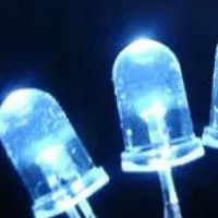
UV LED technology
In the first quarter, UV industry chain enterprises strengthened the research and development of UVC LED technology. Through its exclusive ain UV LED technology, 256nm Japan created UVC led with a luminous efficiency of 50MW, and continuously strengthened the technology to develop 200MW products. The luminous efficiency of 275nm deep UV LED can reach 20MW at 100mA, which has achieved stable mass production; the luminous efficiency of 280nm deep UV LED is 55MW at 350mA; the luminous efficiency of 230nm deep UV LED is 1.6MW at 100mA. In addition, Asahi has cooperated with Nagoya University to develop a laser diode emitting deep ultraviolet light, using specially designed p-side layer to achieve sufficient light limitation and reduce device resistance at the same time, and to suppress light scattering loss by using ain substrate with less defects.
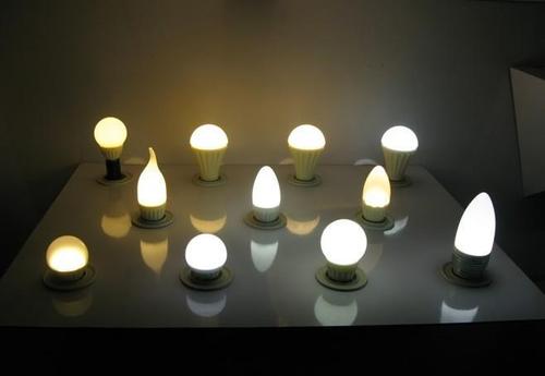
UV LED products
The outbreak of the epidemic has prompted the market of sterilization and disinfection products. Domestic and foreign manufacturers have launched a variety of UV LED products for sterilization and epidemic prevention needs. In addition to UVC LED packaging and modules, UV LED sterilization robots, sterilization sweeping robots, sterilization sticks, sterilization flashlights and other application end products are in full bloom.
UV LED production line and investment
In terms of production capacity and production line, affected by the epidemic in the early part of the first quarter, the resumption of work was delayed, and the enterprises were affected to a certain extent. With the orderly progress of the national work of returning to work and production, Shenzhen Foreign led enterprises said that the order volume increased significantly compared with the same period last year.
In terms of investment, enterprises in the industry have increased investment in the field of deep UV semiconductor, and leading companies in the field of domestic first-line manufacturers and deep UV LED are expected to benefit. Zhongke Lu'an phase I 30 million deep UV LED chips project was successfully put into operation, becoming the world's first mass production of deep UV LED production line. Zhongke Lu'an deep UV photoelectric project is located in Zhangze new industrial park of Changzhi high tech Zone. The project is constructed in two phases with a total investment of about 2 billion yuan. At present, the first phase of 30 million chip production line project has been completed and accepted. It is expected to complete the construction of the packaging pilot line on the second floor of the workshop by the end of August 2020. At the same time, the preliminary preparation for the second phase of 300 million chip project will be carried out, and the construction will start in the second half of the year. The project is estimated at 123 million yuan. MuLinSen invested 36.9 million yuan to obtain 30% equity of Shenzhen Zhishan, which is expected to fully benefit from the growth of deep UV market demand in the future.
Introduction of UV LED project
Nanjing, Jiangsu Province and Changzhi, Shanxi Province have introduced UV industrial chain projects one after another, and the project amount has been disclosed to be 900 million yuan. In the investment promotion conference of Sino US science and technology center in Nanjing Pukou Economic Development Zone, the semiconductor materials, chips and related technology application projects with a total investment of 200 million yuan will be committed to solving the technical problems of deep UV chips. The project will have a huge market prospect in the fields of water purification, air, white household appliances and consumer goods, and will be widely used in the fields of radar and detection. Changzhi national high tech Development Zone of Shanxi Province has introduced the third generation semiconductor UV packaging, Gan epitaxy, chip and application R & D promotion project. The project contracting companies are Shanxi Huawei UV Semiconductor Technology Co., Ltd. and Shanxi zhongweixin Semiconductor Technology Co., Ltd., with a total investment of 700 million yuan. They mainly carry out the third generation semiconductor UV device packaging and application, Gan epitaxy, chip production and manufacturing, etc Rate device packaging, including UVC devices, UV sensors, UV detectors, power semiconductors, etc., is widely used in household appliances disinfection, communication and national defense.
Guangdong Hotsoon Photoelectric Technology Co. LTD
Address:Room 201, Building 1, No. 31, Changping Section, Dongping Avenue, Changping Town, Dongguan, Guangdong, China
Cellphone(WhatsApp): 86-13790398509
Email: Mike@fsfortune.com
Guangdong Hotsoon Photoelectric Technology Co. LTD
Address:Room 201, Building 1, No. 31, Changping Section, Dongping Avenue, Changping Town, Dongguan, Guangdong, China
Cellphone(WhatsApp): 86-13790398509
Email: Mike@fsfortune.com